
Start here 1
Estimate trace impedance
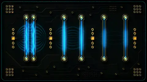
Choose single-ended or differential, then microstrip or stripline, before solving impedance, width, or pair spacing.
Open controlled impedance
Choose the right calculator for controlled impedance, propagation delay, edge-rate bandwidth, wavelength, and first-pass crosstalk checks.
Calculator navigation: Choose the right calculator, follow common design paths, and open supporting pages when the calculation needs engineering context.
Start here
Start from the trace or timing question you need to answer, then follow the calculator and workflow links into solver-backed or measurement checks.
Choose single-ended or differential, then microstrip or stripline, before solving impedance, width, or pair spacing.
Open controlled impedance
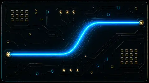
Use effective Dk (Er), velocity factor, delay per length, and trace length to estimate timing.
Open propagation delay
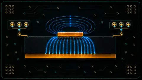
Use geometry or odd/even impedance data to estimate NEXT and FEXT before layout changes become expensive.
Open crosstalk
Estimate signal bandwidth from edge rate before judging electrical length or coupling risk.
Open rise time bandwidth
Calculators
Use these calculators for controlled impedance, timing, wavelength, edge-rate, and crosstalk screening.
Estimate single-ended and differential microstrip or stripline impedance from stackup and trace geometry.
Use when: Use before routing controlled-impedance traces or requesting a stackup from the fabricator.

Estimate PCB trace delay, effective Dk (Er), velocity factor, and delay per length.
Use when: Use when timing, skew, electrical length, or trace-length matching matters.
Estimate near-end and far-end crosstalk from simple geometry or odd/even-mode impedance data.
Use when: Use after edge rate and coupled routing length make spacing rules worth checking.
Convert signal rise time to approximate bandwidth, or bandwidth to rise time.
Use when: Use before deciding whether a trace is electrically short or needs transmission-line treatment.

Convert frequency, period, velocity, wavelength, and wavelength fractions.
Use when: Use to relate signal frequency and velocity to electrical trace length.

Convert amplitude or power ratios to and from dB with percentage context.
Use when: Use when comparing crosstalk, attenuation, margin, or gain/loss ratios.
Workflows
Use these paths when trace geometry, timing, edge rate, or coupled routing affects the next PCB layout decision.
Start from edge rate, then check wavelength, impedance, delay, and crosstalk.
Use width, spacing, stackup, and odd/even estimates before moving to solver or fabricator data.
Questions
Use these answers to choose the right first-pass calculator and the next verification step.
No. It is a first-pass screening calculator. Use the PCB fabricator stackup, solver-backed impedance data, coupons, or measurement for release decisions.
PDN target impedance is a power-integrity rail target from voltage droop and transient current. Controlled trace impedance is a signal-integrity transmission-line property from geometry and stackup.
For digital edges, rise time is often the better first check because crosstalk and transmission-line behaviour follow edge rate, not just clock frequency.
These calculators support early PCB layout decisions. Real controlled-impedance and high-speed designs still need fabricator stackups, field-solving, discontinuity review, SI simulation, coupons, and measurement before release.