

Next check
Propagation delay calculator
Use effective dielectric constant and velocity context to estimate trace delay and length timing.
Estimate first-pass characteristic impedance for single-ended and differential PCB traces across microstrip and stripline geometry modes.
Estimate first-pass PCB controlled impedance from trace geometry and laminate Dk (Er).
Single-ended mode calculates characteristic impedance, effective dielectric constant (Er or Dk), velocity factor, and delay per length. Microstrip mode treats an external trace over one reference plane and estimates effective dielectric constant (Er or Dk) from W/H.
Tolerance range: 59.28 to 75.26 Ω
Use metres as the natural unit for dimensions. Values such as 150µ, 0.15m, and 35µ are accepted where supported by the engineering parser.
Single-ended microstrip estimate.
Impedance and propagation context
Transmission-line parameters per mm
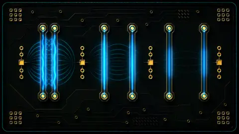
PCB signal integrity
Controlled impedance depends on both the signal structure and the reference-plane geometry. This calculator separates single-ended versus differential traces from microstrip versus stripline construction so those decisions stay visible.
Estimate Z₀, effective dielectric constant (Er or Dk), velocity factor, propagation velocity, and delay per length for one trace over or between reference planes.
Add pair spacing to estimate differential impedance, odd-mode impedance, even-mode impedance, common-mode impedance, and coupling coefficient.
Use microstrip for external traces over one plane. Use stripline for internal traces between two planes under a homogeneous dielectric assumption.
The calculator uses closed-form quasi-static PCB transmission-line estimates. It can solve impedance, trace width, or differential pair spacing where the selected mode supports it.
External traces use an effective dielectric constant because fields travel partly in air and partly in laminate.
Differential mode applies an empirical spacing correction to the single-ended estimate.
Effective dielectric constant also gives first-pass propagation velocity and delay per length.
Unit: Ω
Single-ended transmission-line impedance estimated from the selected geometry.
Unit: Ω
Estimated differential impedance for an edge-coupled trace pair.
Unit: Ω
Mode impedance used by differential signalling and crosstalk workflows.
Unit: Ω
Mode impedance used together with odd-mode impedance to estimate coupling and common-mode context.
Unit: ratio
Equivalent dielectric constant used to estimate velocity for microstrip or stripline propagation.
Unit: Ω/mm
Estimated DC conductor resistance per millimetre from copper resistivity, trace width, and copper thickness.
Unit: F/mm
Derived capacitance per millimetre from the solved characteristic impedance and propagation velocity.
Unit: H/mm
Derived inductance per millimetre from the solved characteristic impedance and propagation velocity.
Unit: ratio
Trace width relative to dielectric height for the selected geometry.
This is a screening calculator. It does not model solder mask, copper roughness, frequency dispersion, glass weave, etch compensation, resin-rich layers, vias, pads, connectors, manufacturing coupons, or impedance-test tolerances.
Use it to start layout and stackup conversations, then confirm with the fabricator and solver-backed data.
These examples show how the same calculator moves between single-ended and differential controlled-impedance checks.
A 150µm external trace over 150µm dielectric on Dk 4.2 laminate gives a first-pass Z₀ estimate and velocity context.
Inputs
Equation and substitution
A first-pass trace-width and stackup estimate.
Confirm with fabricator stackup and impedance solver data.
The same geometry with 150µm edge-to-edge spacing estimates Zdiff plus Zodd and Zeven for coupled-line workflows.
Inputs
Equation and substitution
Early differential-pair width and spacing guidance.
Use solver-backed Zodd and Zeven for critical pairs.
Use these follow-up checks before turning the calculated value into a component choice, layout decision, or production limit.
Use actual dielectric thickness, resin content, copper thickness, solder mask, and Dk from the PCB manufacturer before release.
Closed-form equations are useful for first-pass layout work. Controlled-impedance coupons, solver data, or measurement should drive final release values.
Vias, pads, neck-downs, layer changes, connectors, packages, and return-path interruptions can dominate real impedance even when the straight trace is close.
Use solver-backed Zodd and Zeven values for critical differential pairs and for the engineering mode in the crosstalk calculator.
Follow the next check based on whether the controlled-impedance result affects timing, crosstalk, edge-rate bandwidth, wavelength, or unit conversion.
Use effective dielectric constant and velocity context to estimate trace delay and length timing.
Use odd/even impedance context when moving from spacing rules to NEXT/FEXT estimates.
Feed trace-capacitance estimates into stray-capacitance budgeting for crystal load calculations.
Check edge bandwidth before deciding how carefully a trace must be treated as a transmission line.

Relate operating frequency, wavelength, electrical length, and propagation velocity.

Convert PCB dimensions, SI prefixes, and supporting engineering units.
No. It is a first-pass screening calculator for early stackup and routing decisions. Use the PCB fabricator stackup, solver-backed impedance data, coupons, or measurement for release decisions.
Use microstrip for an external PCB trace over a reference plane. Use stripline for an internal trace between reference planes under a mostly homogeneous dielectric assumption.
Single-ended mode estimates characteristic impedance for one trace. Differential mode also uses pair spacing to estimate differential impedance, odd-mode impedance, even-mode impedance, common-mode impedance, and coupling context.
Use it to start the conversation and sanity-check geometry. Final widths should come from the actual manufacturer stackup, etch compensation, solder mask assumptions, copper thickness, impedance tolerance, and solver or coupon data.
No. PDN target impedance is a power-integrity rail target from allowed voltage droop and transient current. Controlled trace impedance is a signal-integrity transmission-line property from stackup and trace geometry.