
PCB high-speed trace timing and crosstalk workflow
A high-speed PCB check is not a single impedance number. Timing, electrical length, return path, impedance, and coupling all interact, and each step needs the right calculator context.
Reviewed 4 July 2026
Quick answer
What is the practical order for a first-pass high-speed PCB net check?
Start from edge rate, convert that into bandwidth and electrical-length context, estimate propagation delay, check controlled impedance, then screen crosstalk sensitivity before asking a field solver, SI simulation, or measurement to confirm the final design.
Model summary
First-pass model summary
Use these equations, assumptions, and variables as the shared model behind the guide before moving to the worked example and linked calculators.
First-pass bandwidth from 10%-90% rise time.
One-way propagation delay from trace length and signal velocity.
Propagation velocity as a fraction of the speed of light, set by the effective dielectric constant.
Rule of thumb: treat the trace as a transmission line when one-way delay exceeds one-sixth of the rise time.
Variables and natural units
These symbols match the guide equations and use the same engineering-unit conventions as the linked calculators.
BW: Signal bandwidth
Unit: Hz
Equivalent bandwidth implied by the signal rise time; drives transmission-line and crosstalk checks.
tr: Rise time
Unit: s
Signal 10%-90% rise time; shorter rise time means higher effective bandwidth.
tpd: Propagation delay
Unit: s
One-way signal delay along the trace from source to load.
L: Trace length
Unit: m
Physical length of the routed trace.
vp: Signal velocity
Unit: m/s
Propagation speed of the signal on the PCB trace; typically 60-70% of the speed of light.
c: Speed of light
Unit: m/s
Free-space speed of light: approximately 3 × 10⁸ m/s.
εr,eff: Effective dielectric constant
Unit: -
Effective relative permittivity of the substrate and surrounding materials seen by the trace.
Model boundary
- Edge rate often matters more than clock frequency when deciding whether a trace is electrically short.
- Propagation delay and wavelength link the signal to physical trace length and skew.
- Controlled impedance is a transmission-line geometry result, while crosstalk depends on spacing, coupled length, return path, and edge rate.
- PDN target impedance is a neighbouring power-integrity concept, not trace characteristic impedance.
Worked example
1 ns edge on a 75 mm PCB trace
This example estimates propagation delay and checks whether the trace length makes transmission-line treatment necessary.
Inputs
- Edge rate
- 1 ns (10% to 90%)
- Trace length
- 75 mm ≈ 3 in
- Propagation delay
- ≈150 ps/in (FR4 microstrip estimate)
Equation and substitution
Propagation delay
tpd = 450 ps one-way
Delay-to-rise ratio
0.45 — transmission-line treatment required
Next check
Calculate controlled impedance and check whether coupled length warrants a crosstalk analysis.
Calculator workflow
Work through these calculators in order for a complete first-pass check.
-
Step 1
Rise time bandwidth calculator
Estimate the signal bandwidth implied by the edge rate.
Open calculator -
Step 2
Frequency period and wavelength converter
Relate the signal to electrical length and propagation context.
Open calculator -
Step 3
Propagation delay calculator
Estimate trace delay, velocity, and skew context from geometry and dielectric assumptions.
Open calculator -
Step 4
Controlled impedance calculator
Screen single-ended or differential trace geometry before layout release.
Open calculator -
Step 5
PCB NEXT and FEXT crosstalk calculator
Estimate spacing sensitivity and coupled-length risk from a first-pass model.
Open calculator
Guide sections
Keep signal integrity and power integrity separate
Use controlled impedance and crosstalk tools for transmission-line behaviour. Use PDN target impedance only as adjacent rail-noise or power-integrity context. They are related design conversations, but they are not the same quantity and should not be substituted for each other.
What the calculator sequence does not replace
Once the routing matters, move to the actual stackup, fabricator data, field solving, SI simulation, and measurement. The calculator sequence is deliberately a screen for the next layout decision, not a sign-off method.
When does a trace need impedance control?
The common screening threshold for transmission-line behaviour is when the one-way propagation delay exceeds about one-sixth of the signal rise time. Beyond this point, reflections from impedance mismatches can be significant and the trace should be treated as a controlled-impedance transmission line.
For example, a trace with a one-way delay of 500 ps on a board with 150 ps/in propagation delay is about 3.3 inches long. If the edge rate is 1 ns, the threshold is 1 ns / 6 ≈ 167 ps, so this trace well exceeds the threshold and should be impedance-controlled.
Even traces below the threshold benefit from consistent impedance geometry near connectors, vias, and high-frequency devices, because localised discontinuities can reflect or absorb signal energy even on nominally short nets.
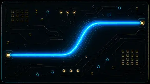
Return path continuity
A signal trace is only half of the current path. The return current flows through the reference plane directly beneath the trace. Any gap, slot, or plane change in the return path forces the return current to travel around the discontinuity, increasing loop inductance, radiating EMI, and potentially coupling into adjacent nets.
Uninterrupted reference planes beneath high-speed traces are the single most effective layout practice for signal integrity. When a trace must cross a plane split or a via transitions a layer, the return current needs a nearby stitching capacitor or return-current via to provide a local path.
Power and ground planes should not share the same layer unless the board is deliberately designed as a power-ground pair in the stackup. Mixing signal return and power distribution on the same plane layer is a common source of EMC and SI problems.
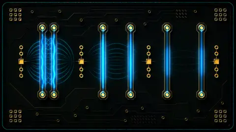
Differential pair routing
Differential signals benefit from tightly coupled routing because the field from the positive signal partially cancels the field from the negative signal, reducing emissions and susceptibility. For effective differential noise cancellation, the two traces must be matched in length and impedance.
Match the trace lengths to within the skew budget specified by the protocol. Many serial interfaces specify maximum intra-pair skew in picoseconds or fractions of a UI. Length matching to within 0.1 mm typically contributes less than 1 ps of skew, but via placement and routing topology also contribute.
The differential impedance target (typically 85-100 Ω for PCIe, USB, LVDS, and similar) is set by both the trace width and the inter-trace spacing. Obtain the target geometry from the fabricator's impedance test results for your specific stackup.
Common mistakes
- Starting with clock frequency only and ignoring the edge rate that actually drives transmission-line behaviour.
- Using PDN target impedance as if it were trace characteristic impedance.
- Trusting a calculator result as a substitute for solver-backed or measured SI verification.
When the model breaks down
- These are first-pass engineering estimates; the sequence does not replace field solving, SI simulation, or measurement on real hardware.
- Discontinuities, vias, connectors, packages, return-path gaps, glass weave, and fabrication tolerance can dominate the real result.
Further checks and references
- Review the real PCB stackup, solder mask, copper thickness, etch compensation, and fabricator impedance tolerance before final routing.
- Check connector launches, vias, reference-plane transitions, and return-path continuity in addition to straight-trace geometry.
- Use the PCB signal-integrity hub and crosstalk calculator for adjacent checks, then confirm critical nets with solver-backed or measured data.
- Confirm the PCB stackup, dielectric constant, and copper weight with the fabricator before committing impedance-critical trace geometries to the layout.
- Check that all signal return-current paths are complete and uninterrupted, especially at plane transitions, splits, and via pad reliefs.
Related calculators
Controlled impedance calculator
Check trace or pair geometry against the target impedance.
PCB NEXT and FEXT crosstalk calculator
Screen spacing and coupled-length sensitivity.
PCB signal integrity calculators
Return to the PCB signal-integrity hub for related timing and routing checks.
FAQ
At what point does a PCB trace behave like a transmission line?
A common screening rule is when the trace delay exceeds about one-sixth of the signal rise time. Use the rise-time bandwidth and propagation delay calculators to check this before routing critical nets without a controlled impedance target.
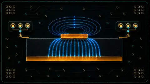
What is the difference between NEXT and FEXT?
Near-end crosstalk (NEXT) is the coupled noise measured at the same end as the aggressor driver. Far-end crosstalk (FEXT) is measured at the far end of the coupled line. They have different dependences on edge rate and coupled length and need to be checked separately for differential and single-ended nets.
Can a trace impedance calculator replace a field solver for production sign-off?
No. Calculators give first-pass estimates from idealised geometry. Real impedance depends on fabrication tolerances, copper roughness, solder mask, fibre weave effects, and adjacent features. Use the calculator for initial screening and confirm critical nets with the fabricator, a solver-backed model, or TDR measurement.